

Face ID and fingerprint sensors make unlocking your phone quick and convenient. You might also use biometrics to approve purchases, access banking apps, or sign in to accounts. So, when your phone suddenly stops recognizing your face or fingerprint, the problem can disrupt more than your lock screen. Sometimes, a simple setting or dirty sensor […]

EBest Circuit at Canton Fair 2026 Autumn
The five-day exhibition has successfully concluded for EBest Circuit at Canton Fair 2026 Autumn. From October 15 to 19, 2026, our team welcomed visitors at Booth 16.3H18 in Area C of the China Import and Export Fair Complex in Guangzhou. This year, our exhibition focused on PCB assembly (PCBA), giving customers a closer look at […]
Wire Harness Classes, Inspection and Testing
IPC 620 is the commonly used name for IPC/WHMA-A-620, the requirements and acceptance standard for cable and wire harness assemblies. It addresses workmanship in wire preparation, crimped and soldered connections, connector assembly, and associated inspection and testing. For a production order, the useful reference is not simply “IPC compliant”: it is the agreed revision, product […]
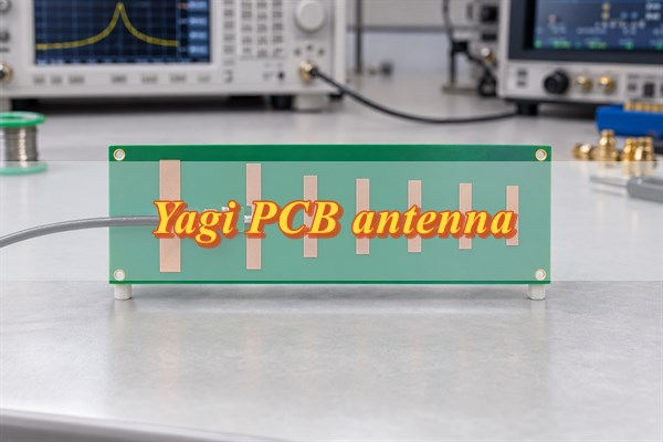
Design, Impedance Matching & Testing
A Yagi PCB antenna uses printed conductive elements to concentrate RF energy in a specific direction. Its performance depends on element dimensions, PCB materials, feed structure, and impedance matching. Small changes in these factors can shift the resonant frequency, reduce gain, or distort the radiation pattern. For a 2.4 GHz Yagi PCB antenna, good impedance […]
Thickness, Prepreg & PCB Stackups
1080 Glass Cloth is a lightweight, plain-woven glass reinforcement used in electronic laminates and PCB prepregs. Published supplier examples weigh about 47–49 g/m², with dry-fabric thickness around 0.05–0.06 mm. Its thin construction helps engineers build closely spaced copper layers without using a heavier glass fabric. However, a PCB does not use the dry-cloth dimension as […]
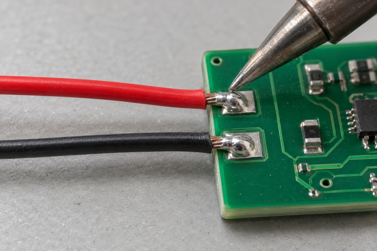
Soldering Wires to PCB for Secure Connections
Soldering wires to PCB pads or plated holes requires a clean, wetted joint and support that keeps cable movement away from the connection. The method changes with the connection point: a wire laid onto a surface pad needs different positioning from one inserted through a plated hole. In either case, adding more solder cannot compensate […]
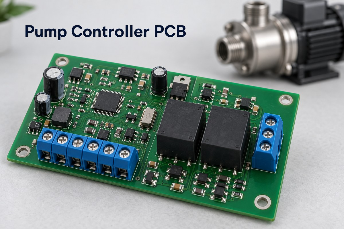
Pump Controller PCB for Reliable Water Pump Operation
A pump controller PCB receives operating signals and controls when a water pump starts, stops, or changes speed. Its role depends on the system: a tank-filling controller responds to water level, a pressure booster responds to demand, and a variable-speed pump may need a power stage as well as control logic. These boards share a […]

The Risks of Using Public USB Charging Stations – The Lab
Your phone battery hits 5% while you’re traveling, shopping, or waiting at the airport. Then you spot a free USB charging port nearby. Problem solved, right? Maybe not. Public USB charging stations offer a convenient way to power up your phone, but plugging your device into an unfamiliar USB port can introduce security risks. Before […]
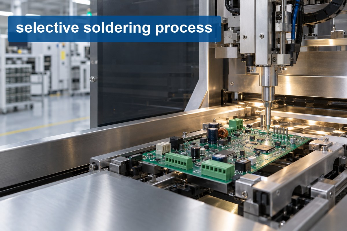
Selective Soldering Process for Consistent Joint Quality
The selective soldering process creates through-hole solder joints only at programmed locations on a PCB assembly. It is commonly used after SMT reflow when connectors, relays, transformers, terminals, switches, or other plated through-hole components still need to be soldered without exposing the entire underside of the board to a full solder wave. Its advantage is […]
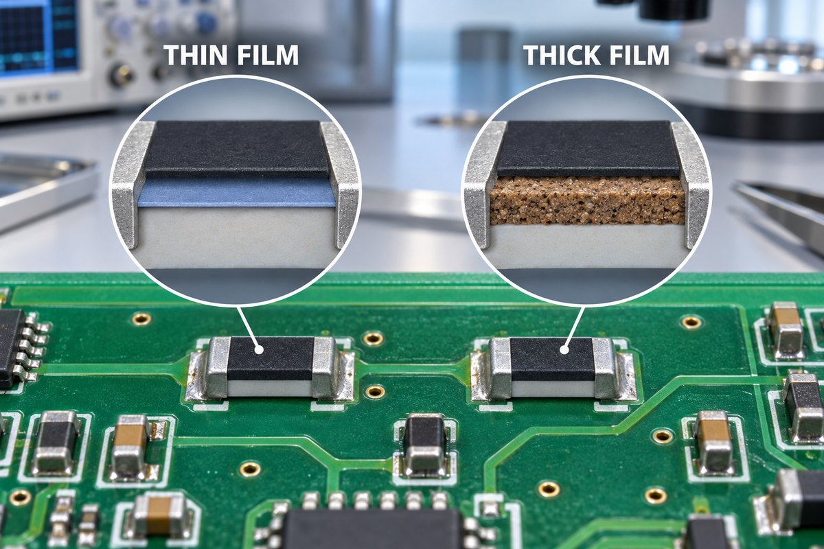
Thin Film vs Thick Film Resistor: Which Fits Your Circuit?
Thin film vs thick film resistor selection affects how accurately a circuit performs after temperature, load, and operating time begin to change. Two chip resistors may have the same nominal value and package but differ in temperature coefficient, noise, long-term drift, pulse behavior, and price. Choosing the appropriate technology helps the assembled board reproduce the […]